
ITEM SPECIFICS
-
Brand
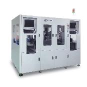
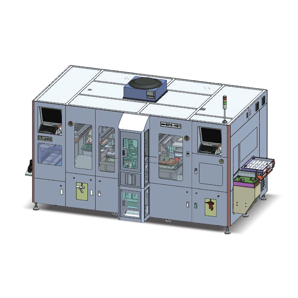
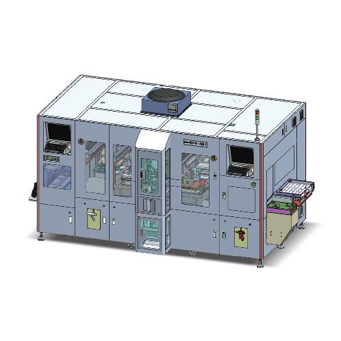
Model BPS-HybridSSP
-
origin
Republic of Korea
-
Size(Capacity)
Strip 50–95 mm (W) × 180–260 mm (l)
-
Function
Strip Handling SiP package
PRODUCT DESCRIPTION
System Performance
Application : Strip Handling SiP package
Handling capability : Strip 50–95 mm (W) × 180–260 mm (l) cycle time / UPH : 45 sec
Yield : 99.98%
Placement accuracy : ± 15 ㎛
min. Solder Ball Diameter : Ø60 ㎛
min. Pitch : 125 ㎛
Warpage capability : max. 10mm for Substrate
Handling capability : Strip 50–95 mm (W) × 180–260 mm (l) cycle time / UPH : 45 sec
Yield : 99.98%
Placement accuracy : ± 15 ㎛
min. Solder Ball Diameter : Ø60 ㎛
min. Pitch : 125 ㎛
Warpage capability : max. 10mm for Substrate
Rework : additional Rework m/c is Required
Tooling conversion time : ≤ 20 minutes
PATENT
˙ Ball grid array Solder Ball mount System
˙ Integrated circuit Package Solder Ball mount method and its following System
˙ Integrated circuit Package Solder Ball mount method and its following System
˙ Ball Supply System in terms of Ball Dispenser
˙ Inline System for marking and Ball mounting in terms of Semiconductor manufacturing Process
˙ Solder Ball mount Equipment Standard Value modi cation method and computer readable recording medium
˙ Solder Ball Bumping Unit and its covering Wafer Bumping Equipment and it using Bumping method
˙ Solder Ball Bumping Unit having assembly means and its covering Wafer Bumping Equipment and its using Bumping method
PAYMENTS DETAILS
This supplier supports payments for offline orders
- Telegraphic Transfer : T/T
- Name : Lee,gyouho
SHIPPING
Shipping from :
Republic of Korea
- , 인천광역시,
-
- Business Type :
- Manufacturer
-
- Main Product :
-
- Established :
- 1996-01-01
Please suggest a variety of your ideas such as design, impact, enhancements, etc
Captcha Required
Please enter the text on the left image to prevent automatic input.
0 / 4000
질문이 없습니다.
CUSTOMER REVIEWS (0)

COMPARISON TO SIMILAR ITEMS more
- No Items
- supplier level
-
 SILVER
- SSP Seller's Store
- Seller's Store url
- Response Level
★ ★ ★ ★ ★

- Supplier Level
★ ★ ★ ★ ★
- Transaction Level
★ ★ ★ ★ ★
SUPPLIER BEST